The Signal Transfer Company

Compact Blameless Power Amplifier

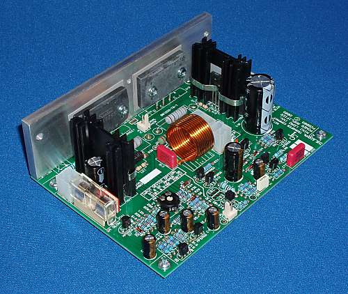
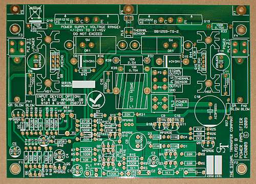
The Compact Blameless power amplifier has been introduced to offer an economical and space-efficient Class-B amplifer that gives all the benefits of Blameless performance. It is mainly intended for use with loads that are nominally 8 Ohms but will still give excellent performance into lower impedances. If you are planning to drive 4 Ohms and below on a regular basis then the Load Invariant amplifier will give improved linearity.

Compact Blameless Power Amplifier assembled

  • Exceptionally low distortion into a wide range of load impedances.
  • Very low noise, due to innovative feedback design.
  • Unique enhanced-tempco bias generator gives excellent control of the critical quiescent conditions.
  • Operates to full specification over a wide range of supply voltages without modification.

  • PCB 009: £27:00 each

F EA T U R E S

  • Output devices can be either TO3P or the larger MT200 package.
  • Alternate positions are provided for the input transistors (Q1,Q2 or Q101,Q102) so that devices with differing pin-outs may be used without having to cross their legs.
  • Tall components have been placed so as not to obstruct screwdriver access when mounting the output devices.
  • Pads and tracking for a heatsink-mounted thermistor have been included. This will connect directly to the Signal Transfer Protection PCB.
  • Full overload and short-circuit protection.
  • Mechanical fixing arrangements improved.
  • Comprehensive project notes included. The overlay includes mechanical dimensions for machining from flat bar an aluminium block for mounting the output devices.
  • Optional input bootstrapping to raise input impedance.

Compact Blameless Power Amplifier PCB

P C B

  • The PCB is now double-sided PTH, so wire links have been eliminated.
  • All transistor positions have emitter, base and collector marked on the top-print to aid fault-finding.
  • Board fixing holes and pads provided for easy mounting of TO3P output devices to a heatsink.
  • High-quality double-sided plated-through-hole PCB
  • Gold-plated pads
  • Solder mask both sides, full screen print with component values included on the silk screen to aid assembly.
  • Double-thickness 2-oz copper to minimise ground resistance and voltage drops.
  • Wire connection points can be either via connectors or by direct soldering.
  • Fully RoHS compliant.
  • Board size 140 by 100 mm overall.

S P E C I F I C A T I O N S

  • Power output: from 25W to 100W into 8 Ohms, depending on supply voltage. Assumes adequate heatsink.
  • Power supply: +/-24V to +/-45V *
  • Distortion: Less than 0.0006% at 1kHz, 25W/8R. Less than 0.003% at 10kHz, 25W/8R.
  • Noise out: Less than -95 dBu (22-22kHz bandwidth, RMS, source resistance 50R)
  • Gain: 23 times (+27.2 dB)
  • Frequency response: +/-0.1 dB, 10Hz - 20kHz
  • Input impedance: 2.2k without bootstrapping, 10k with bootstrapping option
* The Compact Blameless Power Amplifier PCB will operate correctly, in that it gives a visually undistorted sinewave output, from supply rails of +/-5V or lower. This means that initial testing can be done at minimal risk by slowly winding up a variable mains transformer. The amplifier will not of course meet its full performance specifications at such a low voltage.

Compact Blameless Power Amplifier THD graph
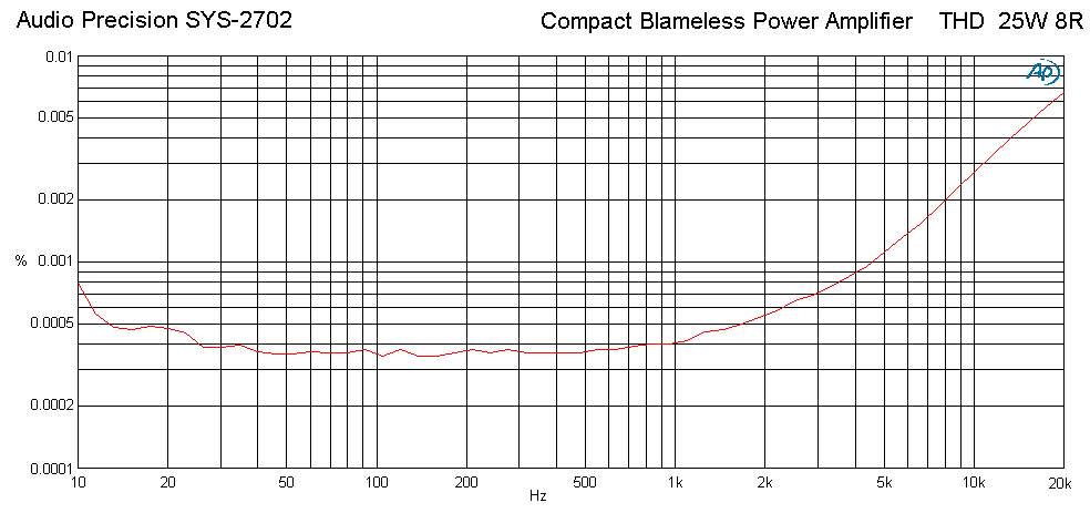
This graph shows the typical amplifier THD when running from +/-24V minimum supply rails. Performance at higher supply rails is somewhat improved.

Measurement system:
Audio Precision SYS-2702.

Measurement bandwidth:
80 kHz, RMS sensing